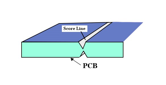


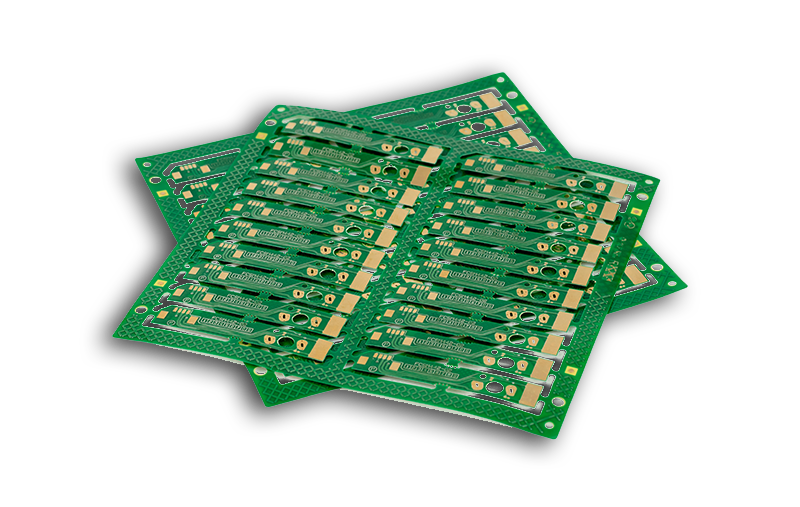

On PCB Drill Size, When makes electronic devices from scratch, you will eventually have to make a few holes. It was only a few decades ago when everyone used simple drills to make their PCB holes. People moved their boards into position and then pulled a lever to start drilling. They then moved the board to the next post and repeated the process.
They used whatever drill bit they had on hand. These drill racks were large with just about every standard drill bit, and deviations from these standard bits issued an upcharge.
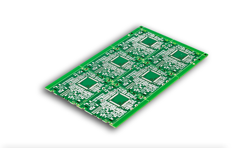
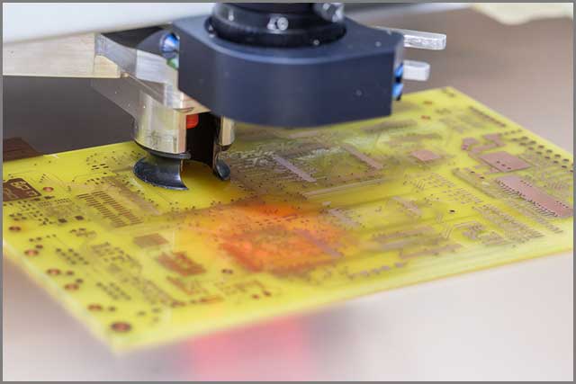
Over time, the size and complexity of PCB assemblies made traditional drilling methods impossible. Now, we have standard PCB drill sizes to make the process easier. These bits fit nicely into classic automatic CNC machines, allowing for effective and consistent printed circuits.
In this guide, you will learn about the size of the drill and how to choose the size of the training that meets your needs.
PCB Drill Sizes
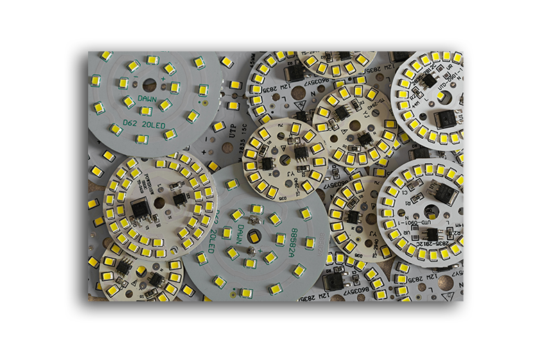
Today’s PCBs tend to have more than 10,000 drill holes of varying sizes. While modern, automated CNC tools let you use any drill size you w0.ant without extra effort, standard drill sizes make it a relatively simple process.
Preparing a blank PCB requires an understanding of the finished product’s purpose, construction, and maintainability. Not all PCBs are thick enough to handle every drill bit out there. It would help if you kept your drill sizes under your board’s aspect ratio or the ratio between its thickness and recommended drill hole size.
For example, a 3 to 1 (3:1) aspect board is 0.062 inches thick and can withstand 0.020-inch diameter drill holes.
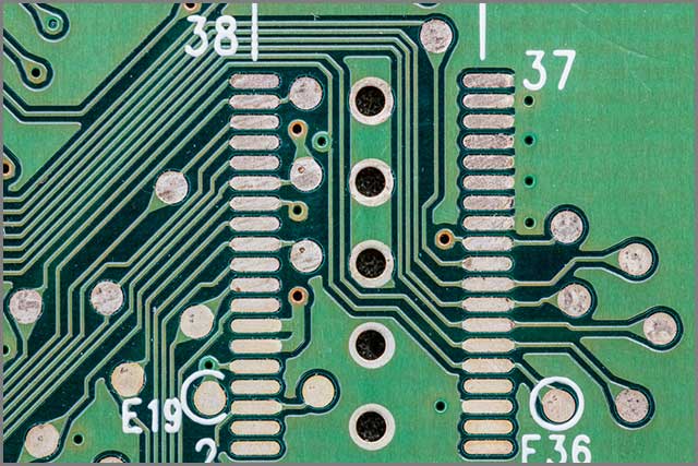
Beyond the aspect ratio, the vias also determine the drill sizes you need. PCB vias plated through holes) come in all shapes and sizes, depending on the complexity of the circuit. You can use laser drills to make the small ones up to 0.006 inches, but most builds will require small “micro vias” cut from a CNC machine. You also need multiple size drills because some vias will go partly through if your project must use multiple board layers.
Therefore, you want PCBs with pre-built standard PCB drill sizes, or at least have a few standardized bits around if you plan to drill your board yourself. It is because everyone will want them.
If you build PCBs for a client, your client will demand those standard sizes and specifications to make adjustments as needed.
Non-professionals will find standard sizes easier to work with, giving you an upper hand.
Standard PCB Drill Sizes
Fortunately, PCB manufacturers provide a wide selection of available drill and hole sizes. Some charge for each used drill size used, but many will offer standard sizes to no change.
Some of these standard sizes include:
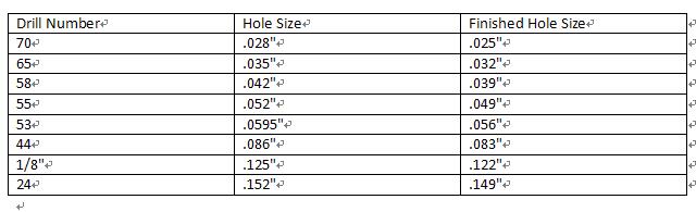
Despite the above chart being in inches, the PCB standards specification expresses drill sizes in millimeters.
While you may work with all of these sizes at one point, you may not need them in all projects. If your drills are too small, you will not fit all your components on the board. If you use bits that are too large, you will waste solder and board area. You may also run into other problems, including stuffing.
The general tip is to make your holes 0.3 millimeters (mm) wider than your component. For example, if your piece is 0.4 mm, you need drill holes as large as 0.7 mm in diameter.
It would help if you also considered the specification standards for your boards. For the SSS specification, you must have no more than 500 holes on your board. The maximum is 2000 holes for DSS.
PCB Drill Size–PCB Design
These specifications are the heart of a good PCB design. They provide the thinness and standard components you should use for a project. However, they are just one aspect of a good PCB design.
Whether you make them in a home tech lab or a professional setting, PCB design starts with an exemplary schematic and goes from there.
It would be best if you created your project’s schematic circuit diagram long before you start buying your board, components, and drill bits. This diagram will serve as your blueprints as you work through the project, laying out traces, vias, drill holes, and everything else your circuit will need.
While making your schematic, you should start with your components before you draw your wires. An exemplary schematic will stick to standard schematic symbols, but you can use any characters you want as long as you are consistent and make your signs public.
Either way, you must consider the footprints and purposes your components need.
PCB footprints define a component’s physical presence on the board. It also sets where you must place your copper pads or through holes.
A component’s purpose is what it does for the entire project. You can place pieces with related goals in the same area to reduce the lengths of your traces. It would help identify these area groups as linearly as possible, creating a direct path flow from one section to the next.
Once you figure out your components and their footprints, you can finish your diagram with the wires and labels for all the symbols. You will eventually copy these labels to their appropriate spots on the board. So, you want to make them easy to understand and read.

3.1 PCB Shape and Size
PCBs come in all shapes and sizes, but you want them as small as possible most of the time. Along with the component footprints, other factors may affect the size you need.
If you place your PCB in an enclosure, the enclosure may define its dimensions.
You might also consider the physical depths of your components as well. For instance, while surface-mounted details are usually small, through-hole parts are often significant but are more accessible to solder.
Because your board may also require several user interfaces such as power connections, potentiometers, LEDs, and audio jacks, your board must be big enough and thick enough to hold them in place.
3.2 PCB Drill Size—PCB Layers
Vias, so copper-plated holes connect these layers into a single circuit, though you can also make this connection through a component. THOUGH EXTENSIVE COURSES ONLY USE SINGLE LAYERS; a PCB can have multiple layers connected via holes and plates. You still may need separate layers if your traces would intersect otherwise.
Still, other projects may reserve a layer for grounding. Typically, the bottom layer, these ground layers, are just copper plates that stretch the entire dimensions of the board.
PCB Drill Size–Drill Size in PCB Design
A lot of PCB design is the placement of the components. They are the heart of your device, providing its functionality, but you must place them somewhere. That would not be a problem if these components did not take the physical space, including how they attach to your circuit board.
Drill size forms a large part of this. Any hole you drill into your board will remove the surface area you could otherwise use for a component’s footprint. Therefore, you want to design your circuit so your drill holes will not cause any problems during assembly.

You can do this by designing with a standard set of drill bits in mind, or you can use components that match the sizes you already have. Each method has its benefits and challenges.
While using the drill sizes you already have will save you money on CNC equipment, you may find getting the right-size components to use complex or impossible. With a standard set, you can reasonably presume any part you have will fit your holes and stay affixed to your board.
Recommended PCB Drill Sizes
So, what drill sizes should you get for your project?
To answer that, you must understand your needs. While it is easy to say you should use standard parts, what is considered standard can change depending on the project type. Beyond that, you may not need everything in the standard.
Your first consideration should be your PCB’s aspect ratio. This ratio between the board’s thinness and the recommended drill size is the critical piece for choosing the correct dimensions, especially if your project must stay within a particular aspect range.
Another thing you should consider is the board’s construction. Some materials can only withstand some sizes and bits without cracking. For instance, the most common type of fiberglass (FR4) boards require tungsten carbide drill bits. Fiberglass eats standard high-speed steel (HSS) bits quickly. So, you can only use significant (>2mm) HSS bits on them if you cannot use carbide ones. It is because carbide tips are expensive and brittle. You need an excellent vertical drill stand if you need bits that are smaller than 1mm.
As most of your projects will use carbide bits, bit style will also come into play. Carbide bits come in straight-shank and compressed shank formats. Straight shank bits keep the same size along their entire shaft. Meanwhile, thick, turbo, or reduced shank bits tapper down to some standard length. Straight bits are perfect for holes below 1mm in diameter as they do not break as quickly as the reduced ones. They are also typically cheaper as well.

It would help if you next considered your project’s components’ lead diameters. The leads of your electrical components set the required sizes for your drill holes. If you cannot attach a part to your board, you cannot use it in your circuit. Fortunately, most components have standard lead diameters.
Some of these diameters include:
- ICs, resistors – 0.8m
- Larger diodes (1N4001 and so on.), square-pin headers, D connectors, IDC connectors, TO-220 leads, and so on.- 1.0mm
- Terminal blocks, trimmers, and so on. 1.2 to 1.5mm
Most projects will rarely need holes sizes smaller than 0.8 mm in diameter. Thus, 0.8 mm should be the lower bound on your drill sizes. So, you want at least two 0.8mm drill bits in your rack since small bits tend to be brittle and break easily. 1.0mm and more significant bits are more resilient, but you should always have at least one spare just in case.
You also want to make sure your holes are about 0.007 mm larger than your leads. For example, resistors with 0.022-inch leads require holes around at least 0.029 inches in diameter.
How to Calculate
Now that you know what to consider when decided on the appropriate drill sizes for your PCB project, you can start calculating the sizes you need. Although it sounds challenging, if you know where to start, the process is straightforward.
6.1 PCB Drill Size—Find the Maximum Lead Diameter
Before you do anything else, you should have already picked out your project’s electrical components. Therefore, their leads are a great place to start. You want to find the element with the thickest leads and measure their diameters. You will find the lead diameter of your components on their datasheets or packaging.
6.2 Calculate the Minimum Hole Size
With the maximum lead diameter in hand, you can calculate the minimum hole size.
Minimum Hole Size is calculated according to equations:
- 1.Minimum Hole Size = Maximum Lead Diameter + 0.25mm (for Level A of IPC-2222)
- 2.Minimum Hole Size = Maximum Lead Diameter + 0.25mm (for Level A of IPC-2222)
- 3.Minimum Hole Size = Maximum Lead Diameter + 0.25mm (for Level A of IPC-2222)
6.3 Calculate the Pad Diameter
You step to calculate your pad diameters using your minimum hole size. To do this, you need the minimum annular ring or the smallest pad area surrounding your project’s vias. For most projects, this value should be 0.05mm or 50 micrometers.
It would be best if you also decided on your acceptable fabrication allowance. While you want your values close to ideal, there will always be some errors and deviations in your drilling. Your fabrication allowance is how much of this deviation your project can withstand without causing problems. According to the IPC-2221 Standard Specification, your budget should never be smaller than 0.6mm for Level A, 0.5mm for Level B, and 0.4mm for Level C.

Once you collect all this information, you can calculate your PCB’s pad sizes by:
Pad Diameter = Minimum Hole Size + Minimum Annular Ring X 2 + Minimum Fabrication Allowance
- 1.Pad Diameter = Minimum Hole Size + 0.1mm + 0.60mm (for Level A of IPC-2221)
- 2.Pad Diameter = Minimum Hole Size + 0.1mm + 0.50mm (for Level B of IPC-2221)
- 3.Pad Diameter = Minimum Hole Size + 0.1mm + 0.40mm (for Level C of IPC-2221)
For example, with a lead diameter of 0.55mm:
- Level A Pad Diameter: Minimum Hole Size = 0.80mm; Pad Diameter = 1.50mm
- Level B Pad Diameter: Minimum Hole Size = 0.75mm; Pad Diameter = 1.35mm
- Level C Pad Diameter: Minimum Hole Size = 0.70mm; Pad Diameter = 1.20mm
6.4 PCB Drill Size—Differences between density levels A, B and C
If you got this far, you might be wondering about the A, B, and C levels. The IPC-2221 standard calls for three different component placement densities.
Density Level A is the most preferred specification level among PCB manufacturers. It defines the General Design Producibility Standard, calling for both low-component density and maximized footprint geometries.
Level B defines the Moderate Design Productivity Standard. As the default standard for all PCB projects, you can use it for reflow, wave, drag, or dip soldering. It called for median footprint geometries, providing robust solder attachments.
Level C defines the High Design Productivity Standard. Also called a Reduced Level, C allows for high component densities with small footprints. Hand-held and portable devices typically use the Level C Standard.

PCB Drill Size–Conclusion
When created a PCB application from scratch, you must drill a few holes. Blank PCBs do not come pre-punched, and you cannot affix everything to the surface. Whether it is for soldering joint or vias, drilling is just a part of a PCB assembly. However, like in any other CNC project, you cannot use any drill bit. Instead, it would help if you only used drill sizes that match the needs of your components and project in general.
While you could calculate your required bit sizes, you can get much leverage by ensuring that you use standard drill sizes in your project. The correct drill sizes will let you securely affix everything to your board without wasting space or solder. If you need help deciding on what sizes you need for a project, contact us right away. Our expert technicians will help you evaluate your project specifications to select the right size and style bits for your needs.